

Materials

GO film in hydrated condition
- Rich microstructural detail of hydrated GO films is captured in real time, with fine textures and internal architecture clearly visible.
- Enables dynamic analysis of morphology and film behavior in native conditions.

Crystalline Defects in MOFs
- Structural heterogeneity and crystalline defects are directly revealed, capturing transitions from ordered lattices to disordered domains.
- Enables rapid, label-free assessment of morphology and defect distribution critical for understanding function in real-world MOF materials.

Crystals as They Grow
- Real-time growth of crystals at oil–water interfaces and in microemulsions is visualised from nucleation to microstructure, with shape controlled by surfactants.
- Enables label-free, time-resolved imaging of crystallisation processes in native environments for materials science, pharmaceuticals, and food research.
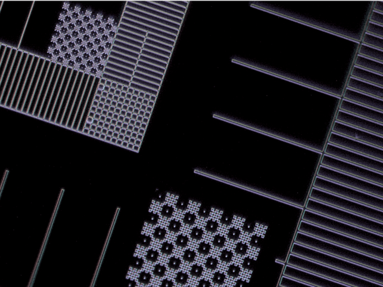
Seeing through Semiconductors
- Crisp nanoscale gold patterns on silicon wafers are revealed in air or liquid without conductive coatings, enabling accurate visualisation of edge features and pattern fidelity.
- Enables high-resolution, label-free inspection of semiconductor surfaces for defect detection and quality control during fabrication and prototyping.

Security Printing
- Fine details in embedded diffraction gratings and 2D flakes are exposed in complex polymer films, even with reflective or transparent features.
- Enables wide field, non-destructive imaging of anti-counterfeit elements in banknotes and security materials under varied lighting and wear conditions.